-250x250.jpg)

-250x250.JPG)


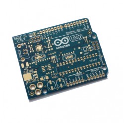
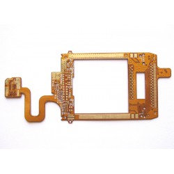
PCB Prototype


-500x500.JPG "PCB Prototype")


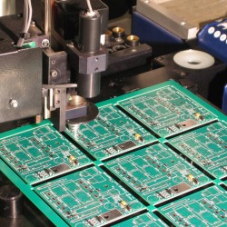
- PCB are produced by the biggest PCB manufacture in China, there are more than 5000 kinds of boards produce per day in the factory.
- All prototyping PCBs will be tested by a flying probe to make sure all vias are connected. To make sure that all tracks and pads are connected,all PCBs will also get a 100% Automated Optical Inspection.
Reviews from our customer:
- Price is transparent and has no hidden cost,you can get a instant quote by selecting the options above according to your PCB specification.
- Shipping at affordable prices save your money too. You can get an instant shipping cost in "shipping estimate",there are different price and delivery time of shipping methods to meet your requirement.
- The Manufacturing time will be 4-6 days for 2 layers board and 5-7 days for 4 layers board. We also provide 48 hours rush PCB prototyping service.
Lead Time 1 or 2 Layers 4 Layers 6 Layers Normal 4-6 days 5-7 days 9-10 days Rush 48 Hours 72 Hours 72 Hours
- 3-7 work days by DHL/UPS express and 8-20 work days by Air mail are available. 95% customers said they received thier boards on time.
- Select the options according to your PCB specification and upload your Gerber files then add to cart and checkout
- You can track your order in your order history or on the track order page just with your order number and email address .
- Gerber files are recommended. Gerber files must be RS-274x format. Drill file(pcbname.TXT) should be Excellon format, and make sure it include drills size and position data.
Outline
pcbname.GML
Drill & Holes
pcbname.TXT
Solder Paste Top
pcbname.GTP
Top Layer
pcbname.GTL
Solder Paste Bottom
pcbname.GBP
Layer 2
pcbname.GL2
Solder Mask Top
pcbname.GTS
Layer 3
pcbname.GL3
Solder Mask Bottom
pcbname.GBS
Layer 4
pcbname.GL4
Silk Screen Top
pcbname.GTO
Layer 5
pcbname.GL5
Silk Screen Bottom
pcbname.GBO
Bottom Layer
pcbname.GBL
- We also accept PCB files generated by Eagle,Altium Designer,PADS.
- Make sure your pcb design comply with follow limits.
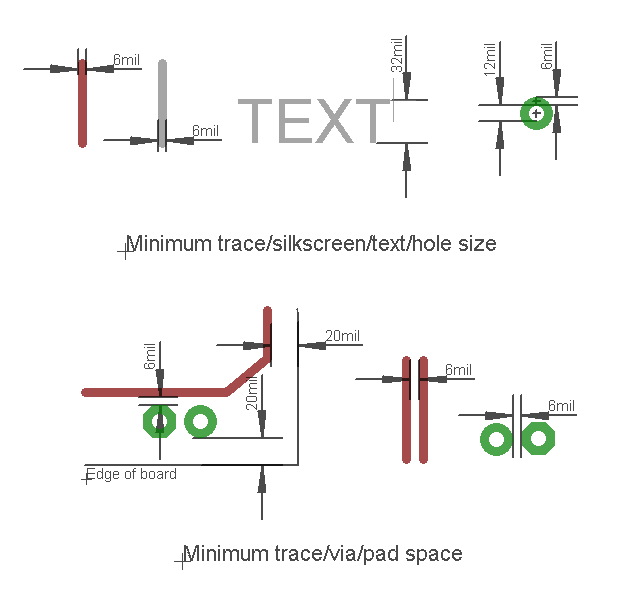
- Also,you can import the design rules files into your EDA software to design your PCBs.
- Design rules and CAM: Eagle PCB design rules and CAM
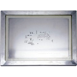
Solder Paste Stencil:
The Solder Paste Stencil also known as SMT Stencil, is Laser-cut steel on a aluminum frame with a minimum recommended pitch of 0.4mm.This Solder Paste Stencil are custom-made for your PCB using your Gerber or CAD files.With SMT Stencil,you can make your PCB assembly job easier and save your time.
You can get a separated solder paste stencil without PCBs in solder paste stencil product page.
*Please make sure the effective area is twice as big as your PCB so that top and bottom side can be placed on the same stencil.
| Effective Area | Total Size | Price | Weight |
13.0 x 21.0 cm | 30.0 x 40.0 cm | $19 | 1.9kg |
19.0 x 29.0 cm | 37.0 x 47.0 cm | $20 | 2.0kg |
| 19.0 x 29.0 cm (Frameless) | 28.0 x 38.0 cm (Frameless) | $18 | 1.0kg |
24.0 x 34.0 cm | 42.0 x 52.0 cm | $28 | 2.4kg |
| 22.0 x 40.0 cm | 40.0 x 60.0 cm | $32 | 2.7kg |
| 22.0 x 60.0 cm | 40.0 x 80.0 cm | $34 | 3.8kg |
27.0 x 37.0 cm | 45.0 x 55.0 cm | $36 | 2.8kg |
37.0 x 47.0 cm | 55.0 x 65.0 cm | $44 | 3.9kg |
38.0 x 38.0 cm | 58.4 x 58.4 cm | $44 | 3.6kg |
Please send the correct Gerber file to pcb@shenzhen2u.com asap, we will use the Gerber file if we have not start to process the order. But we can not change/cancel your order if the factory already put it on manufacturing line.
Please leave a message "There is no solder mask/ drill hole/ silkscreen" when you check out.
| Layers | Thickness(mm) | Stackups |
| 4 | 1.6 | 1oz+2116(0.12mm)+FR4(1.2mm)+2116(0.12mm)+1oz |
| 1.2 | 1oz+2116(0.12mm)+FR4(0.8mm)+2116(0.12mm)+1oz | |
| 1.0 | 1oz+2116(0.12mm)+FR4(0.6mm)+2116(0.12mm)+1oz | |
| 0.8 | 1oz+2116(0.12mm)+FR4(0.4mm)+2116(0.12mm)+1oz | |
| 6 | 2.0 | 1oz+2116+FR4(0.8mm)+2116+FR4(0.8mm)+2116+1oz |
| 1.6 | 1oz+2116+FR4(0.6mm)+2116+FR4(0.6mm)+2116+1oz | |
| 1.2 | 1oz+2116+FR4(0.4mm)+2116+FR4(0.4mm)+2116+1oz | |
| 1.0 | 1oz+1080+FR4(0.4mm)+1080+FR4(0.4mm)+1080+1oz | |
| Prepreg 2116 Thickness 0.12mm, 1080 Thickness 0.06mm | ||
0.2 mm or 8 mil for 4 layers .
0.25mm(10mil)
8x8cm
layer 46, but you need to add a note there
1*2mm
No, V-cut line can only be straight line.
layer 50, but you need to add a note there.
The production time is the manufacture time, it does not include the checking time, packing time and shipping time.
PCB Capabilities
| Item | Specs | |
| PCB Prototype | Premium PCB | |
| Material | FR-4 | FR-4,FR-4 (High Tg), Aluminate core,FLEX |
| Number of layers | 1, 2, 4, 6 | 1~20 |
| Available Board Thickness | 0.6(4 layer except), 0.8, 1.0, 1.2, 1.6, 2.0 | 0.2, 0.4, 0.6, 0.8, 1.0, 1.2, 1.6, 2.0, 2.5, 3.0, 3.5, 4.0 |
| Special Process | NO | Blind vias,Buried vias,Half vias, Impedance control |
| Thickness Tolerance | (t >= 1.0) ± 10% | (t >= 1.0) ± 10% |
| Thickness Tolerance | (t < 1.0) ± 0.1mm | (t < 1.0) ± 0.1mm |
| Minimum trace width | 0.1016mm/4mil | 0.076mm/3mil |
| Minimum trace/vias/pads space | 0.1016mm/4mil | 0.076mm/3mil |
| Minimum copper to board edge clearance | 0.3mm | 0.25mm |
| Minimum silkscreen width | 0.1524mm/6mil | 0.1524mm/6mil |
| Out Layer Copper Thickness | 35~70um/1~2oz | 35~140um/1~4oz |
| Inner Layer Copper Thickness | 17um/0.5oz | 17~70um/0.5~2oz |
| Drilling Hole(Mechanical) | 0.2 ~ 6.35mm | 0.2~6.35mm |
| Finish Hole(Mechanical) | 0.2 - 6.35mm | 31.50 - 250.00 |
| SMT min Solder Mask Width | 0.1mm/3.94mil | 0.1mm/3.94mil |
| Min Solder Mask Clearance | 0.13mm/5.12mil | 0.1mm/3.94mil |
| Max PCB Dimension | 40mm*40mm | 1016mm*610mm |
| Aspect Ratio | 8:1 | |
| Solder Mask Type | Photosensitive ink | |
PCB stackup:
| Layers | Thickness(mm) | Stackups |
| 4 | 1.6 | 1oz+2116(0.12mm)+FR4(1.2mm)+ |
| 1.2 | 1oz+2116(0.12mm)+FR4(0.8mm)+ | |
| 1.0 | 1oz+2116(0.12mm)+FR4(0.6mm)+ | |
| 0.8 | 1oz+2116(0.12mm)+FR4(0.4mm)+ | |
| 6 | 2.0 | 1oz+2116+FR4(0.8mm)+2116+FR4( |
| 1.6 | 1oz+2116+FR4(0.6mm)+2116+FR4( | |
| 1.2 | 1oz+2116+FR4(0.4mm)+2116+FR4( | |
| 1.0 | 1oz+1080+FR4(0.4mm)+1080+FR4( | |
| Prepreg 2116 Thickness 0.12mm, 1080 Thickness 0.06mm | ||
2-170x170.jpg "Breadboard (165×55mm whtie)")
Breadboard (165×55mm whtie)
Features:800 Tie Points Self-adhesive Can be interlocked for larger projects 2 powe..
$6.80

Solder Paste Stencil
The Solder Paste Stencil also known as SMT Stencil, is Laser-cut steel on a aluminum frame..
$18.00

Part Sourcing
If you want us to do Part sourcing and PCB assembling ,please use our PCB Assembly service instead. ..
$1.99

PCB Assembly
Easy to quote and order PCBAFill out the form to get instant estimate PCBA quote Upload the B..
$49.90

Premium PCB Quote
Descristion If you need more special process for your boards ,such as blind vias, FPC..
$0.00

